
Abstract
Many renewable energy sources such as solar and wind energy are grown and well developed as the cost effective solution being widely used in Nigeria but the whole Africa and world at large has witnessed a dramatic increase, concern over environment and demand of energy have led the world to think about alternate energy sources such as wind, hydro, solar and fuel cells. The voltage multiplier cell was incorporated with the interleaved converter to design the DC to DC boost converter for the PV application. The proposed converter is supplied by 18V as an input voltage and produces 99V output and gives 95 % of efficiency under no load and 94% under load conditions. The performance of the proposed topology was substantiated and the results achieved from the fabricated prototype are in good agreement with the design strategies. The effects of input parameters such as sun radiation and useful power input on PV system and DC-DC converter outputs were exploration for 14 days. Results confirmed that the DC-DC converter was perfectly designed and accurately constructed, when integrated with solar PV system, data were captured under no load and on load conditions.
Author Contributions
Academic Editor: Alireza Heidari, Tenure of Chemistry at California South University.
Checked for plagiarism: Yes
Review by: Single-blind
Copyright © 2024 Abubakar Hafs Musa, et.al
 This is an open-access article distributed under the terms of the Creative Commons Attribution License, which permits unrestricted use, distribution, and reproduction in any medium, provided the original author and source are credited.
Competing interests
The authors have declared that no competing interests exist.
Citation:
INTRODUCTION
Many renewable energy sources such as solar and wind energy are grown and well developed as the cost effective solution being widely used in many applications 1. These energy sources are preferred for being environmental friendly. Solar energy has become one of the most promising sources of energy due to the fact that solar energy is clean, free of charge, sustainable and less pollution. The PV power generated widely under the distributed mode in both standalone and grid-connected applications, for the economic development of any country, energy is one of the major 6. The majority of energy is used in form of electricity and a huge amount of electric energy is required by the world to fulfill daily demand, PV panel is scalable and easy to integrate with existing power converters 2. Normally, PV panels generate voltage ranging from 12 V–75 V which cannot be utilized for grid or off-grid applications 4. A power converter can be used to step-up the efficiency of the power generated from the PV panels, and it can also be used to charge batteries.
Power electronics converters serve as interface between user loads and the source. The converters are classified into AC-AC, AC-DC, DC-AC and DC-DC converters. The classification is based on nature of the input source and output load. For instance, a DC-DC converter is used to connect a dc input source to a dc load 5.
The DC/DC converters are widely used in regulated switch mode DC power supplies. The input of these converters is an unregulated DC voltage, which is obtained by PV array and therefore it will be fluctuated due to changes in radiation and temperature 7. The utilization of such energy sources is constrained by interfacing devices required to conditioned power from the sources and make it suitable for user loads. DC–DC converters and inverters have been designed and used for interfacing photovoltaic with the load 3.
The determination of the efficiency of electronics devices for interfacing renewable energy systems is a very crucial issue. The fact that the cost for energy may be higher than conventionally produced electricity. However, the efficiency of the DC-DC boost converter is obtained by using equation III 1.
Useful power input = sun radiation in W/m2 * Area of the PV module in m2
 (I)
(I)
The measured voltage and current output from the PV panel are usually used in equation 1.1 and 1.2 to determine the total power output generated by the PV module.
 (II)
(II)
 (III)
(III)
Efficiency =  (IV)
(IV)
Simulation/experimental analysis of the proposed converter are presented and discussed in details. To verify the performance of the proposed converter, a laboratory set-up was prepared and tested. Figure 1
Figure 1.Graphical representation of the system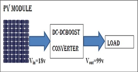
MATERIALS AND METHOD
MATERIALS
The proposed new converter was design with two inductors (L1 & L2), four diodes (D1, D2, D3& D4), two capacitors (C1& C2), two power switches (Q1 and Q2), and a resistor (RL). The actual sizes of the electronics components for the designed of the DC-DC boost converter based on simulation are shortlisted in Table 1.
Table 1. Components specifications used in the design| S/N | COMPONENTS | Specifications |
|---|---|---|
| 1 | Input voltage Vin | 18V |
| 2 | Inductor L1 | 80µH |
| 3 | Signal generator (MOSFET) | IRF520 |
| 4 | Inductor L2 | 80µH |
| 5 | Diodes D1, D2, D3& D4 | 1N400G |
| 6 | Resistor RL | 1kohms |
| 7 | Capacitor C1 | 220µF |
| 8 | Capacitor C2 | 33µF |
| 9 | Output Voltage Vout | 99V |
METHODOLOGY
The proposed circuit diagram of the DC-DC boost converter is integrated with voltage multiplier circuits into a conventional interleaved boost converter. The converter which consists of a power input source, 2 Inductors, and 2 signal generators, 4 diodes, 2 capacitors and the load resistance was design using Multism 14.2. Figure 1 presents the circuit diagram of the proposed converter. Figure 2
Figure 2.Proposed circuit diagram of step-up DC-DC boost converter topology.
The operation principle of the proposed topology under continuous conduction mode: The steady state operation of the proposed converter (CCM) consists of modes of operation.
The switches Q1 and Q2 are ON and the diodes D1, D2, D3, and D4 are reverse biased. The diodes D1 and D2 are reverse biased due to the voltage of the capacitor C1. The diodes D3 and D4 are reverse biased due to the voltage difference between the capacitor C3 and C1.Figure 3
Figure 3.Proposed circuit diagram of boost converter at mode 1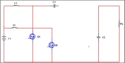
The mode 2 switch Q1 is ON and the switch Q2 is turned OFF. The diodes D1 and D3,maintain a reverse bias state as shown in the figure below. Energy stored in the inductor L1 rises from minimum to maximum. The primary side of the coupled inductr transfers energy to capacitors C1.Figure 4
Figure 4.Proposed circuit diagram of boost converter at mode 2
In mode 3 the switch Q1 is OFF and the switch Q2 is turned OFF. The diodes D2 and D4,maintain a reverse bias state as shown in the figure below. Energy stored in the inductor L2 rises from minimum to maximum. The primary side of the coupled inductor transfers energy to capacitors C1.Figure 5
Figure 5.Proposed circuit diagram of boost converter at mode 3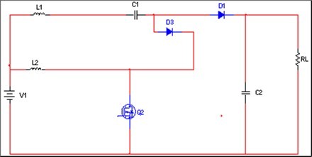
However, when the switches are turned OFF in mode 4, the diodes become forward biased and they stars conducting. Energy stored in the inductor L1 and L2 is already transferred to capacitor C1 in the previous modes and in this mode energy along with source is transferred to capacitor C2 and load. Inductor currents fall from maximum value to minimum value during this period. Figure 6
Figure 6.Proposed circuit diagram of boost converter at mode 4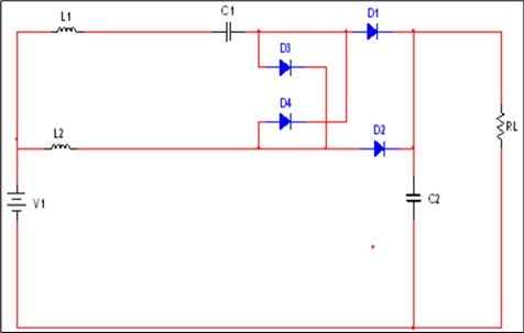
CIRCUIT DESIGN ANALYSIS OF THE DC-DC BOOST CONVERTER
The proposed components sizing for the DC-DC Boost converter design involved the voltage ratings and specifications of all the electronics components as indicated in equations 1 to 17
By applying KVL to classical boost converter when ON we have;

 (1)
(1)
For OFF state classical boost converter, yield
 (2)
(2)
 (3)
(3)
 (4)
(4)
The net voltage across the inductors is equal to zero hence

Equation 4 becomes

 (5)
(5)
Considering equation 1 and 3 for inductor voltages, Using Volt-second balance law;
Equation 1 reads
 (6)
(6)
Equation 3 reads for off state
 (7)
(7)

 (8)
(8)
Integrating over one complete switching frequency with the use of equation 6 and 7

The LHS is zero because in periodic steady state, the net charge in inductor current is equal to zero.

 (9)
(9)
The first part of the equation 9 is for on state and the second part for the off state, putting equation 3 into 9.
 (10)
(10)

 =
=  (11)
(11)
 (12)
(12)
The proposed boost converter is the sum of two classical boost converters. The voltage gain of the proposed converter will be twice equation 12.

 (13)
(13)
 (14)
(14)
The voltage gain of the proposed converter in terms of duty cycle exist as
 (15)
(15)
The duty-cycle becomes
 (16)
(16)
In terms of voltage stress on switch, the voltage stress of the components will be calculated using, equation (17)
 (17)
(17)
Result of the designed circuit
The simulation analyses of the new converter are presented Figure 2, Figure 3, Figure 4, Figure 5. The experiment was done to validate the simulations at such that the corresponding experimental parameters can be evaluated from the theoretical equations. The lists of the parameters used which include their respected values of the proposed converter are analyzed and shortlisted in details as in Table 1
The output and input voltage were recorded, average voltage was evaluated. The input and output voltages across the components were simulated and their graphs were also shown in the Figure 2a, Figure 2b, Figure 2c, Figure 2d.
Figure 2a.Input voltage and output voltage of the boost converter.
Figure 2b.Voltage across the two switch (cQ1 and Q2)
Figure 2c.Voltage across the two inductors (L1 and L2)
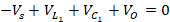
Figure 2d.Voltage across the two capacitors (C1 and C2)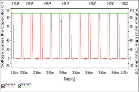
EXPERIMENTAL TEST
The measuring instrument used for investigation the performance DC-DC boost converter are short-listed in Table 2
Table 2. Measuring Instruments for the experiment| Instrument | Specifications |
|---|---|
| Pyronometer | TES 1333R Data logging Solar power meter |
| Multimeter | DT9205A, (0 – 120 V) |
| PV module | 50W AP-PM-50 |
| Solarimeter | PMA2100 |
The direct sun radiation striking the surface area of the PV module has been measured simultaneously with the input and output voltages at intervals of 10 minutes for half a month. The average was collected and results were obtained. The constructed set-up DC-DC boost converter and experimental has been presented in plate 1 and 2. The PV panel specification used in the experiment is shown in Table 3 below:
Table 3. PV module specification| S/N | PARAMETERS | SPECIFICATION |
| 1 | Maximum power (Pmax) | 50W |
| 2 | Output tolerance | +5% 0r -5% |
| 3 | Current at Pmax | 2.86 A |
| 4 | Voltage at Pmax | 17.70 V |
| 5 | Open circuit voltage | 21.50 V |
| 6 | Short circuit current | 3.00 A |
The Constructed DC-DC boost converter is shown in the plate 1, and the experimental set up presented in plate 2.
Plate 1.Constructed diagram of the boost converter
Plate 2.Experimental set up of DC-DC Converter
DISCUSSION
Experimental Test Result
Figure 6: presents a graph of the inter relationship between the useful solar power input and Solar PV power output under no-load conditions. When the useful solar power input has the maximum value of 307.984W the solar PV module generated 45.5249W at 12:00 PM. However, the solar PV module power output has reduced to a lower value of 0W at 7:00PM at the same time the useful solar power input was 1.388W. This indicated that the solar PV module power output depends really on the useful solar power input.
Figure 6.Graph of inter relationship between the useful solar power input and Solar PV power output under no load condition
Figure 7: presents a graph of the correlation between the useful solar power input and Solar PV power output under load conditions. When the useful solar power input has the maximum value of 314.348W the solar PV module generated 45.6896W at 12:00 PM. However, the solar PV module power output has reduced to a lower value of 0W at 7:00PM at the same time the useful solar power input was 2.4W. This indicated that the solar PV module power output depends dully on the useful solar power input and followed the same trend under load condition.
Figure 7.Graph of inter relationship between the Solar PV power outputs against useful solar power input on load condition
Figure 8 presents three-axis graph of inter relationship between the DC-DC converter output and PV Module output voltages against use solar power input under no-load. It has being observed that at maximum value useful solar power input of 307.984W, the PV module and the DC-DC converter outputs voltages have increases to values of 18.89 V and 99.81 V on no load condition respectively at 12:00 pm. This indicated that the voltage outputs from the PV Module and the DC-DC converter dully depends on solar useful power input.
Figure 8.Graph of inter relationship of useful solar power input, output voltage of the converter and PV module under no load
Figure 9 present three-axis graph of inter relationship between the DC-DC converter output and PV Module output voltages against use solar power input under load condition. It has being observed that at maximum value useful solar power input of 314.348W, the PV module and the DC-DC converter outputs voltages have increases to values of 18.88 V and 99.83 V on load condition respectively at 12:00 pm. This indicated that the voltage outputs from the PV Module and the DC-DC converter dully depends on solar useful power input.
Figure 9.Graphs of inter relationship between the DC-DC converter output voltage, PV Module voltage output and useful solar power input on load condition.
DISCUSSION
Figure 2 to Figure 3 represent the input and output signals obtained with a duty-cycle of 64% and 99 V DC output was realized from 18 V DC input. This means that a voltage gain of g = 5.56 is confirmed, and voltage stresses are highly reduced in the components.
Considering the inter relationship between PV output power and net power consumption, as shown in Figure 6 and Figure 7 under no-load and load conditions, the result having a net power was obtained at maximum 307.984 W captured and 45.5249 W produced without load, and with load the PV module withstand 314.348W and generate 45.6896W. These demonstrate that PV output clearly depends on available power consumption, which in turn depends on the intensity of the sun being incident on the PV module. However, the tie up between available solar energy input and efficiency of photovoltaic modules with no-load and load, shown in Figure 8 and Figure 9, this proved proportionality between the three parameters. When the system was unloaded, the graph followed the same trend, showing efficiency slowly increasing at some points and decreases at others as power consumption. This shows that there is a confirmed inter-relationship between the three axis graph as they followed the same trend as in load conditions. Although, the DC-DC converter was able to optimize the 18.89 V from the PV module to 99.81 V at no load, but under the load condition it went from 18.88 V to 99.83 V which increases and also optimized. Moreover, DC-DC boost converter output is shown to be more responsive to net power consumption when the load is connected.
CONCLUSION
A design plan with Power Conversion group is familiar and considered as an alternative to the primarily selected topology. In this research, a step-up DC-DC converter has been proposed. The results obtained shows that the pulse signal used in the new converter provide an extended voltage gain with a high reduction of duty-cycle and voltage stress within the semiconductor components which has been reduced to minimum value compared to other designs. The analysis and experimental results imply that the proposed converter achieves high efficiency within a wide input range and a wide load range including light load. These characteristics have made the new converter ideal for interfacing PV modules and other renewable energy resources.
The 18V to 99V DC-DC boost converter which has been designed constructed and experimentally tested with solar PV module with no load and load condition. Therefore, the boost DC-DC converter may be technically and economically workable to be integrated with photovoltaic systems for energy optimization and hence the demand of energy transition and the quest for reliable, affordable and sustainable energy supply will surely decrease if something of this nature is considered and put in to related applications.
References
- 1.Bako A, Kabiru M, Samaila B, Isah H. (2022) Design and performance evaluation of DC - DC step up SEPIC converter for photovoltaic based off grid application.Journal of Energy Engineering and Thermodynamics.ISSN:. 02, 2815-0945.
- 2.Bolcar K, Ardani K. (2011) International Energy Agency Co-operative Programme on Photovoltaic Power Systems:. Task 1 Exchange and dissemination of information on PV power systems,”National Survey Report of PV Power Applications in the Unites States .
- 4.Fathabadi H. (2016) Novel high efficiency DC / DC boost converter for using in photovoltaic systems.Solar Energy. 125, 22-31.
- 5.Mousavi A, Das P, Moschopoulos G. (2012) A comparative study of a new ZCSDC-DC full-bridge boost converter with a ZVS active-clamp converter.IEEE Transactionson Power Electronics. 27(3), 1347-1358.